

Every advanced AI chip in this data center was born inside an EUV lithography system.
I. The "Magic" of Extreme Ultraviolet Light
To build faster processors, we need smaller transistors. In 2026, we are working with structures so small that traditional light is simply "too fat" to draw them. Imagine trying to paint a masterpiece with a broom—that was the problem with older DUV (Deep Ultraviolet) light.
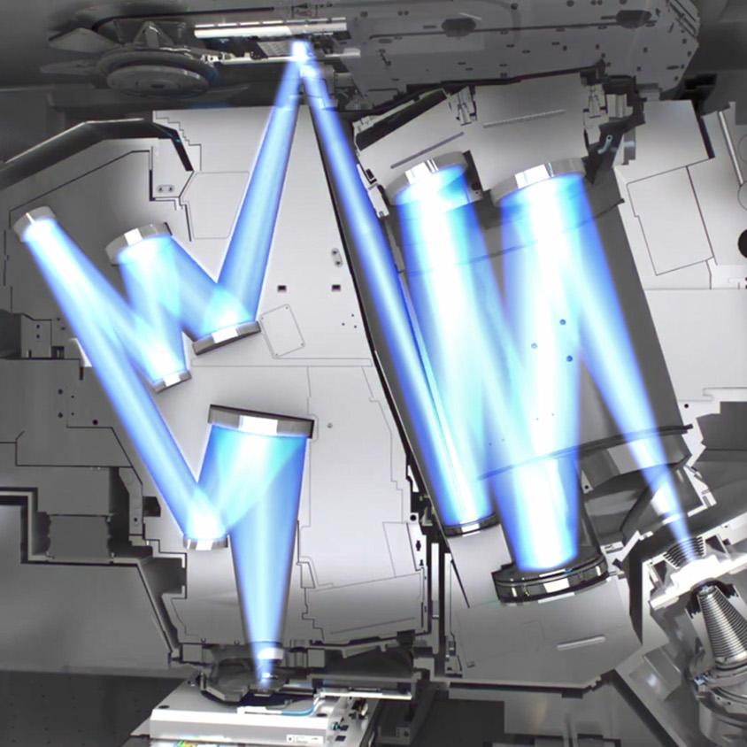
EUV Lithography solves this by using a wavelength of 13.5 nanometers. This light is so close to the X-ray spectrum that it doesn't behave like normal light. It is absorbed by almost everything—including air and glass lenses. This is why an EUV machine must operate in a total vacuum and use mirrors instead of lenses.
II. Creating "Sunlight" in a Box
The process of creating EUV light is one of the most violent acts in industrial engineering:
- Tin Droplets: 50,000 tiny droplets of molten tin are fired through a vacuum every second.
- The Laser Hit: A high-power CO2 laser hits each drop twice. The first pulse flattens it; the second pulse vaporizes it into a plasma.
- Plasma Ignition: This plasma reaches 220,000°C—nearly 40 times hotter than the surface of the sun—emitting the 13.5nm EUV light.
III. The Hidden Innovation: ZEISS SMT
While ASML builds the machine, ZEISS Semiconductor Manufacturing Technology (SMT) builds its heart: the Starlith® optical system. This is where the world's most "hidden" innovations lie.
1. The World’s Flattest Mirrors
Because EUV light cannot pass through glass, ZEISS creates mirrors made of over 100 alternating layers of Silicon and Molybdenum. These are the most precise surfaces ever made by humans.
"If a ZEISS EUV mirror were scaled to the size of Germany, the largest bump on its surface would be only 0.1 millimeters high."
2. High-NA EUV: The 2026 Breakthrough
In 2026, the industry is transitioning to High-NA (Numerical Aperture) EUV. This new generation of machines (the Twinscan EXE series) uses larger, non-spherical mirrors. ZEISS had to invent entirely new sub-atomic measuring systems to verify the shape of these mirrors, as no existing technology was precise enough.
The precision of ZEISS mirrors allows for the transistor density found in modern NVIDIA and Apple chips.
IV. Why It Matters
Without this partnership between ASML and ZEISS, Moore’s Law would have died years ago. Today, EUV technology is a matter of national security. Each machine costs over **$200 million**, weighs **180 tons**, and requires three Boeing 747s to transport.
- AI Supremacy: Only EUV can print the 2nm and 3nm chips required for next-gen AI.
- Energy Efficiency: Smaller transistors mean your phone battery lasts longer and data centers consume less power.
- Geopolitical Leverage: The tech is so complex that it has created a "chokepoint" in the global supply chain.
Explore Further
Watch how light is manipulated at the atomic level in this official breakdown:
For technical whitepapers, visit the official site:
Official ZEISS SMT Website